First ever on-demand atomic layer advanced manufacturing technology based on hybrid Direct Atomic Layer Processing. It is suitable for a wide range of applications such as MEMS, devices, optics, photonics, packaging, RF & electronics and quantum devices which can be developed with ATLANT 3D technology with previously impossible functionality and speed at a fraction of a cost. ATLANT 3D’s Direct Atomic Layer Processing (DALP®) has revolutionized prototyping, turning a traditionally lengthy process into a rapid, precise operation. Key benefits include accelerated development cycles, atomic-level control for complex prototypes, versatile material and surface adaptability, and cost reductions due to increased efficiency. This advancement in DALP® fosters a conducive environment for innovative microdevice fabrication, marking a significant leap in microfabrication technology. We developed DALP® (Direct Atomic Layer Processing) patent-pending technology that provides highly conformal, direct material writing, and removal with atomic precision and material versatility. The evolution of Atomic Layer Processing has been marked by a significant transition, primarily spearheaded by ATLANT 3D’s innovative DALP® technology. This paradigm-shifting advancement redefines the precision and control achievable in thin-film deposition. By facilitating atomic-scale manipulation within the fabrication process, DALP® introduces an enhanced level of granularity and uniformity in material layering. This breakthrough is indicative of a broader trajectory within materials science, driving towards miniaturization and enabling the complex device architectures necessary for next-generation technologies. Sequential pulse sequence for precursor and co-reagent delivery. Time base separation of reagents. TALD is the traditional form of ALD, known for its sequential exposure of surface substrates to precursor vapors, each separated by an inert gas purge to prevent gas-phase reactions. TALD’s strength lies in its exceptional conformality and thickness control, making it ideal for high-quality thin-film coatings. However, TALD’s reliance on vacuum environments and time-consuming purge steps often results in slower deposition rates, which can be a limiting factor for large-scale and rapid manufacturing needs. Spatial separation of precursor and co-reagent with increased deposition speed. Physical distance separation of reagents. SALD, an evolutionary step from TALD, maintains the self-limiting surface reactions characteristic of ALD while enhancing throughput. By spatially separating the precursors, SALD systems deposit materials at atmospheric pressure, significantly increasing the deposition rate. SALD is adaptable to roll-to-roll processes, making it attractive for large-area coatings. Nevertheless, SALD’s dependency on sophisticated equipment to maintain precursor separation can complicate system design and scalability. ATLANT 3D’s Direct Atomic Layer Processing (DALP®) technology represents a seminal breakthrough in the atomic layer deposition (ALD) arena. By ingeniously combining the meticulous precision of Temporal ALD (TALD) with the accelerated deposition rates characteristic of Spatial ALD (SALD), DALP® stands as a beacon of innovation, all while operating in ambient atmospheric conditions. This remarkable synthesis of speed and accuracy in DALP® is made possible through a distinctive microreactor design, which enables the direct application of precursor molecules onto the substrate, negating the need for vacuum environments that have long been a staple of ALD processes. The Direct Atomic Layer Processing (DALP™) technology has been rigorously tested with a variety of Atomic Layer Deposition (ALD) materials. These materials have been chosen for their unique properties and applications in various high-tech industries. The tested ALD materials with DALP® demonstrate the technology’s versatility and efficiency in handling diverse substances, ensuring precision and consistency in the deposition process. This extensive testing underscores DALP® potential in revolutionizing material processing in microfabrication and nanotechnology fields. Used for its photocatalytic properties and UV absorption, common in sensors and solar cells. Offers semiconducting, piezoelectric, and pyroelectric properties, ideal for electronic and optoelectronic devices. A highly conductive and corrosion-resistant metal, often used in electronic components and catalytic applications. Known for its hardness and thermal stability, used in insulating layers and as a barrier material. A p-type semiconductor with applications in batteries, solar cells, and gas sensors. A highly dense and corrosion-resistant material, used in high-temperature and harsh environmental applications. Known for its electrochemical stability, used in electrodes and corrosion-resistant coatings. Exhibits high dielectric constant and stability, used in semiconductor gate insulators and optical coatings. Known for its electrochemical stability, used in electrodes and corrosion-resistant coatings. The selected ALD materials, each with unique properties, affirm DALP’s applicability across multiple domains, including semiconductor manufacturing, energy storage, and nanoelectronics. ATLANT 3D’s technology involves the sequential deposition of gasses for atomically precise patterning of various materials.So far we tested with our technology the following materials: TiO2, Pt, ZnO, SiO2. And it is continuously updated. Our DALP™ technology allows to print conformally different materials, enabling: Our technology allows unprecedented selective patterning on flat, corrugated and porous surfaces: Find insights into our Direct Layer Atomic Processing (DALP®) and other advanced technological developments. Here we explains our pioneering nanofabrication methods, their applications, and advantages in the realm of atomic-scale manufacturing. DALP® TECHNOLOGY
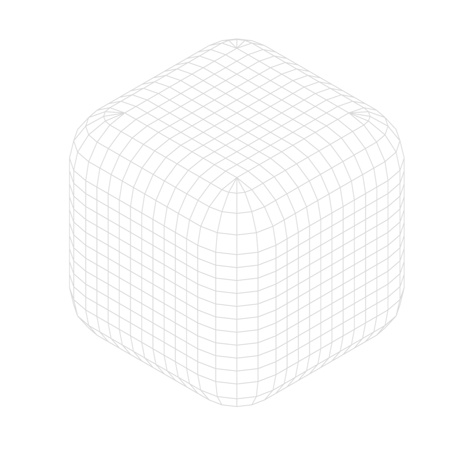
![]() Unique technology
Unique technology REDEFINING MICROFABRICATION
![]() Advanced Microfabrication
Advanced Microfabrication Rapid, Precise, & Versatile Atomic Processing
Innovation
Efficiency
Materials
DALP™
![]() Paradigm-shifting technology
Paradigm-shifting technology EVOLUTION OF ATOMIC LAYER PROCESSING
First there was
TEMPORAL ALD
Then there was
SPATIAL ALD
And now there is
DALP®
![]() Materials
Materials ALD MATERIALS TESTED WITH DALP®
MATERIAL
TiO2 DALP® tested
MATERIAL
ZnO DALP® tested
MATERIAL
Pt DALP® tested
MATERIAL
Al2O3 DALP® tested
MATERIAL
CuO DALP® tested
MATERIAL
Ir DALP® tested
MATERIAL
IrO2 DALP™ tested
MATERIAL
HfO2 DALP® tested
MATERIAL
SnO2 DALP™ tested
GAS DEPOSITION

MULTISTACK PRINTING
COMPLEX SURFACES
Questions & Answers


We developed DALP® (Direct Atomic Layer Processing) patent-pending technology that provides highly conformal, direct material writing, and removal with atomic precision and material versatility.
+50%
10x
450+
Titanium Dioxide
Zinc Oxide
Platinum
Aluminum Oxide
Copper Oxide
Iridium
Iridium Oxide
Hafnium Oxide
Tin Oxide