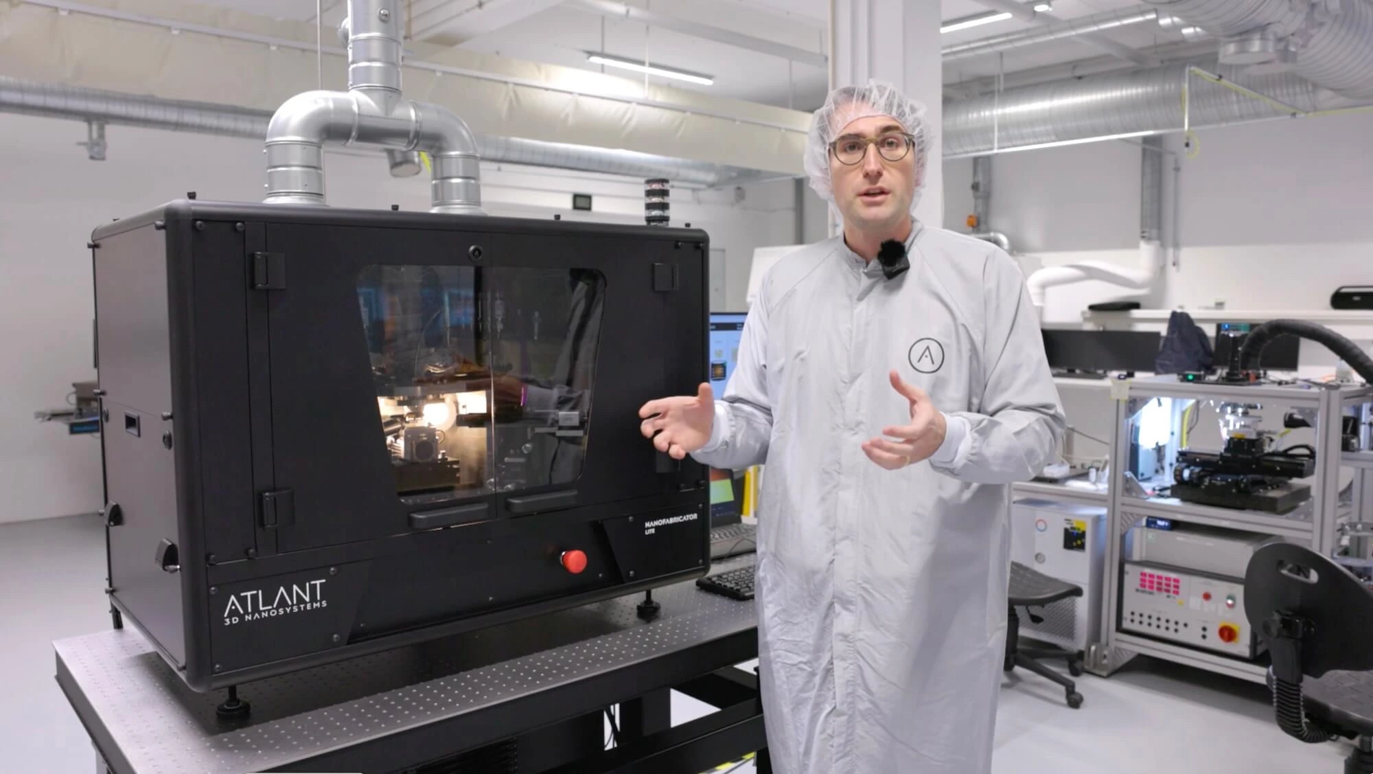
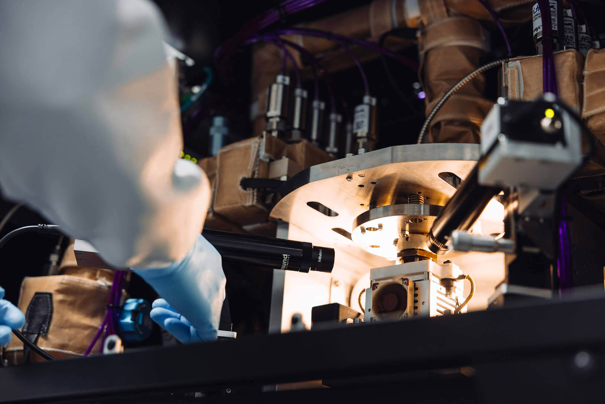
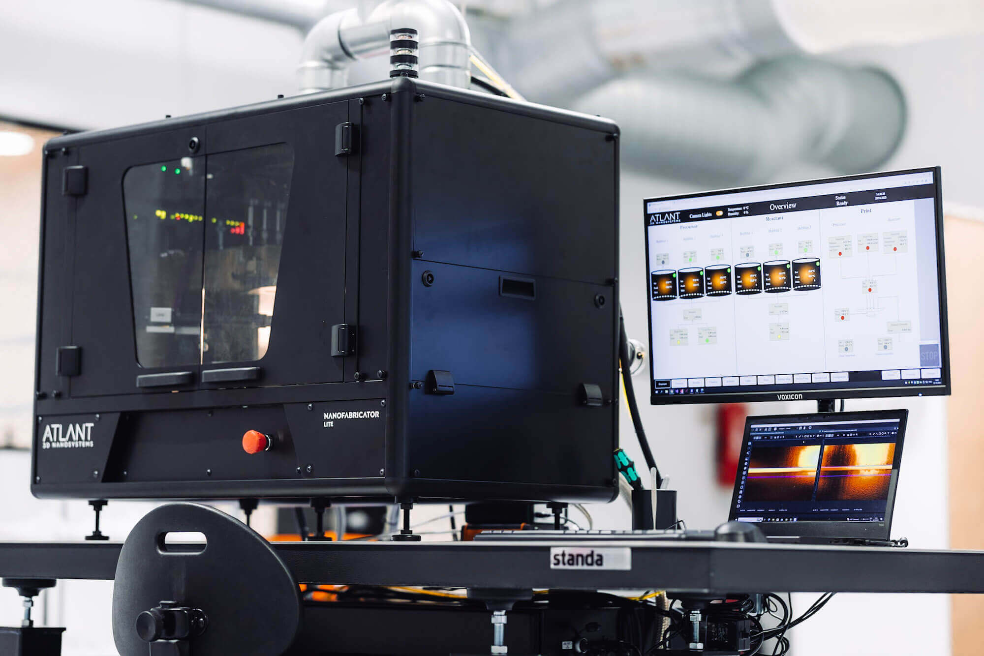
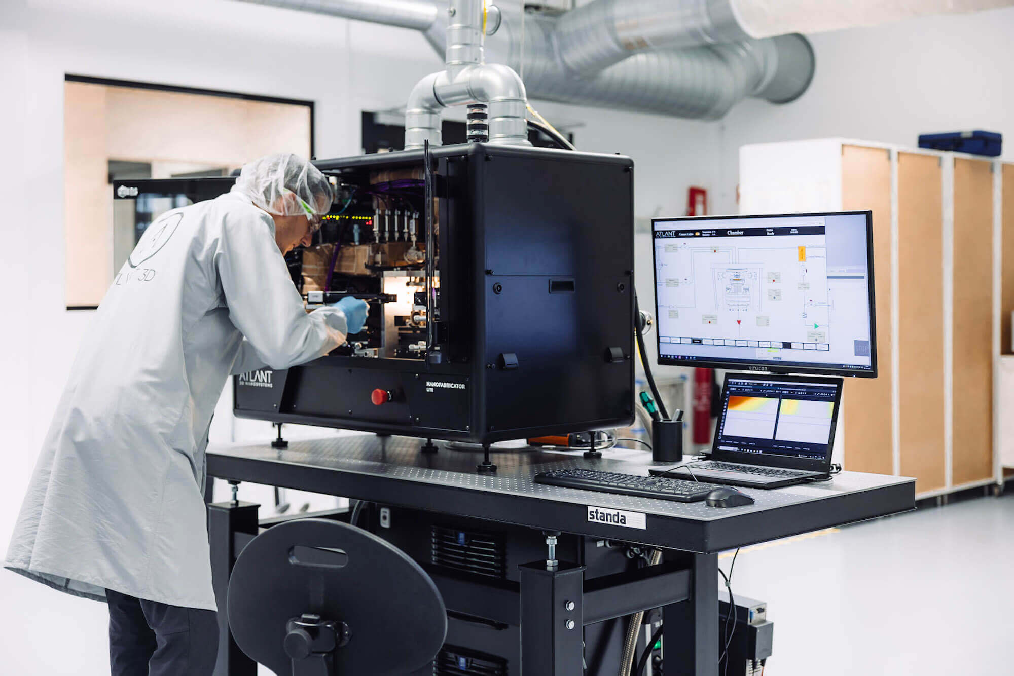
Discover the most versatile & powerful tool ever created to accelerate advanced material innovation, rapid process testing & device development with atomic precision. Experience the unprecedented flexibility & material versatility! We enable on-demand next-generation microdevices printing on simple and complex surfaces atom-by-atom. The NANOFABRICATOR™ LITE is the most compact tool ever created to accelerate materials, processes and device innovation with atomic precision. It is suitable for a wide range of applications such as MEMS, devices, optics, photonics, packaging, RF & electronics and quantum devices which can be developed with ATLANT 3D technology with previously impossible functionality and speed at a fraction of a cost. ATLANT 3D’s proprietary DALP® – DIRECT ATOMIC LAYER PROCESSING technology is enabling a paradigm shift across the whole value chain from advanced material innovation to advanced manufacturing of industrial solutions. The existing standard in the fabrication industry, photolithography-based processes, demand extensive infrastructural support and time. Typically, a minimum of 10 processing loops involving around 40 distinct machines are required, necessitating a large-scale operational setup. The entire process cycle usually extends over a period of at least one month. Furthermore, this method is not without its drawbacks: it poses significant environmental hazards, incurs high capital expenditures (CAPEX) and operational expenses (OPEX), and is characterized by lengthy innovation cycles. This traditional approach, while established, faces challenges in terms of efficiency, sustainability, and agility in response to evolving technological needs. ATLANT3D’s DALP®, or Direct Atomic Layer Processing, streamlines microfabrication by combining multiple processes into one compact machine, reducing processing time to just 1-2 days. Key advantages include: The whole process from experiment design to obtaining samples can take hours with several various DOE parameters. The processed sample has completed DOE with multiple parameter variations including thicknesses, temperatures, and materials. This step involves creating a detailed digital blueprint of the desired pattern. It requires precise design work to ensure that the specifications of the pattern are accurately represented and ready for processing. In this phase, a systematic approach is taken to plan the experiment. It includes defining the process parameters and conditions, setting up the necessary files, and ensuring that all variables are considered for a successful outcome. Here, a blank substrate is loaded into the NANOFABRICATOR™ LITE. This substrate serves as the base material on which the processing will be carried out, according to the predefined digital pattern and DOE parameters. This step signifies the completion of the processing phase. The substrate, now imprinted with the desired pattern through the Nanofabricator’s precise atomic layer processing, is ready for inspection and further use. This final stage involves the core technology of the NANOFABRICATOR™ LITE. It precisely adds or removes material at an atomic scale, following the digital pattern and DOE guidelines, to create the final micro- or nano-structured sample. The NANOFABRICATOR™ LITE enables advanced material innovation, rapid process testing, and device development across multiple advanced applications. It exemplifies a paradigm shift across diverse industrial landscapes. Explore how our cutting-edge equipment is advancing industries by offering precision, efficiency, and versatility in nanofabrication. DISCOVER APPLICATIONS Our patent pending rapid and direct atomic layer processing technology DALP® offers rapid material and process development and testing, maskless process flexibility, and unparalleled prototyping speed, reducing the time of design iterations, resource allocation and cost of innovation. NANOFABRICATOR™ LITE enables multi-material deposition in one process, tested on a wide range of advanced materials, independent of surface roughness and substrate sensitivity with multi-shape deposition and a high degree of thickness control. DALP® represents a quantum leap in process innovation, encapsulating direct patterning with remarkable process flexibility. It advances the understanding of material deposition, addressing the complexities of cross-sectional line profiles and the intrinsic nature of atomic growth. The DALP® excels in the deposition on intricately contoured surfaces, negating the necessity for vacuum environments — thereby streamlining the manufacturing workflow and enhancing the efficiency of material innovation. Staircase with 0.3 nm step height and 3 microns step width. Smooth 1.5 nm height valleys repeated. Tapered shape structure. Characterization of self-limiting surface chemistry and digital growth in DALP®. Thicknesses are determined for two distinct DALP® materials by ellipsometry. Cross-section of platinum deposition for capacitive sensor in the 20 µm channel. The EDX scans shown to the right indicate conformal deposition of platinum along the sidewalls. The DALP® system demonstrates its capacity to engineer patterns with atomic precision, facilitating the creation of complex microscale structures. ALD conformality and low T. deposition enables processing sensitive and rough substrates. Silicon/SiC/GaN wafers. Glass/Fused silica/borosilicates. Polymer. A. “Anodic” aluminum oxide macropores coated with Pt. B. Nanostructured black Si surface coated Pt different thickness. C. Si trench coated with a Pt carbon nanograss. D. Aligned Si trenches coated with a perpendicular line of TiO2 At ATLANT 3D, we are not just changing how things are made; we are redefining the principles of manufacturing. Our commitment to sustainability is a testament to our belief that responsible innovation and business practices can create a positive impact on the world, paving the way for a more sustainable future in manufacturing and beyond. * Dependent on materials to be deposited and customer needs. ** Additional number of bubblers and reactants dependent on customer needs. *** Additional reactant types dependent on customer needs. **** Clean room, CLASS 8 min recommended. ***** Argon recommended. Delve into the comprehensive FAQs to explore the NANOFABRICATOR™ LITE’s capabilities, applications, and technical prowess. From handling diverse substrates to offering customizable features and ensuring precise control, this guide covers everything you need to know about this groundbreaking device. Explore more questions about the NANOFABRICATOR™ LITE, where we delve into its advanced material testing, device structure development, and diverse gas handling capabilities. Learn about its pivotal role in photonics, optics, RF & Microelectronics, and emerging technologies, along with its proficiency in handling complex surfaces. Discover how its ambient processing environment and adaptability make it a perfect fit for both research and production settings, backed by ATLANT 3D’s comprehensive post-purchase support. Explore the NANOFABRICATOR™ LITE’s capabilities, from achieving precise line widths to performing multimaterial stack printing and selective area deposition. Discover its impressive process speed range and ability to handle crystalline material growth, along with direct additive and subtractive processing. NANOFABRICATOR™ LITE

DALP®. ATLANT 3D’s Microreactor Direct Atomic Layer Processing technology offers maskless process flexibility and unparalleled prototyping speed – reducing the time of design iterations, resource dependencies and overall cost of innovation.
Multi-material. Enabling multi-material deposition in one process, tested on a wide range of advanced materials, independent of surface roughness and substrate sensitivity with multi-shape deposition and a high degree of thickness control.
NANOFABRICATOR™ LITE. Suitable for a wide range of applications such as MEMS and sensors, optics, photonics, advanced packaging, microelectronics as well as emerging applications. Designed as a compact and versatile tool to seamlessly integrate into your lab infrastructure.
DALP® Technology
REDEFINING MICROFABRICATION
PARADIGM SHIFTING PROCESS

CURRENT PROCESS
PHOTOLITHOGRAPHY-BASED PROCESS
ATLANT 3D’S PROCESS
DIRECT ATOMIC LAYER PROCESSING

HOW WE DO IT
SIMPLIFYING THE WHOLE PROCESS

PREPARING DIGITAL PATTERN FILE
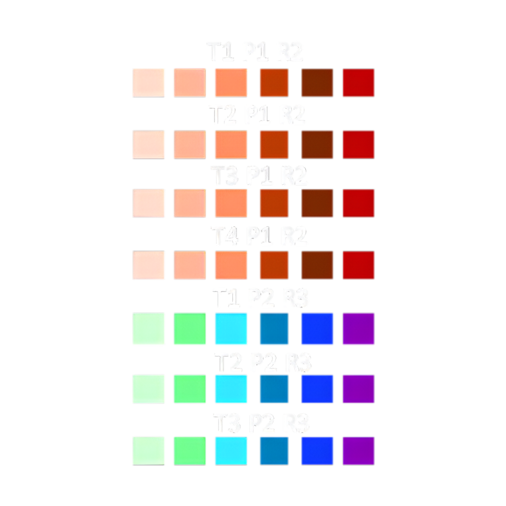
DEFINING DOE PROCESS FLOW AND FILES

UPLOADING BLANK SUBSTRATE

DIRECT ATOMIC LAYER PROCESSING

PROCESSED SAMPLE COMPLETED
Expanding Horizons
Diverse Advanced Applications
DALP® Technology
Rapid, flexible & versatile atomically precise processing
PROCESS INNOVATION INSIGHTS
SURFACE STRUCTURATION


Cross-sectional line profile and growth nature

CONFORMALITY

Direct patterning & process flexibility

SUBSTRATE VERSATILITY

CONFORMALITY

Sustainability
Setting New Benchmarks in Sustainable Manufacturing
Nanofabricator™ LITE
Technical Specification
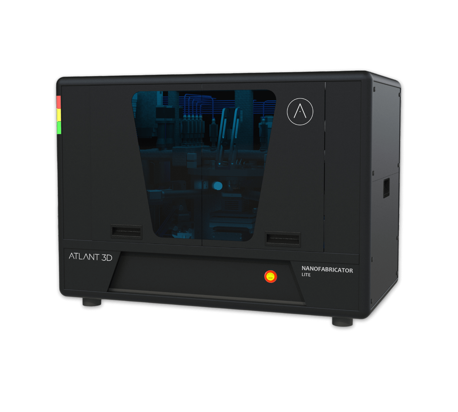
Substrate
Process Chamber
Gas system
Options
Questions & Answers
Capabilities
Specification
- Technology
OUR TECHNOLOGY
TechnologyDiscover ATLANT 3D's unique atomic layer advanced manufacturing technology based on Direct Atomic Layer Processing (DALP®).


- Solutions
OUR SOLUTIONS
All ProductsOur revolutionary tools are built to enhance the whole value chain of advanced micro- and nano-device manufacturing. Our A-HUB solutions enable rapid prototyping, pilots and feasibility studies.
- Applications
ADVANCED NANOFABRICATION
All ApplicationsOur technology is built for advanced applications enabling previously impossible functionality and speed at a fraction of the cost. Its reach across multiple application domains plays a pivotal role in propelling industries toward cutting-edge technological achievements.
- Insights
INSIGHTS
Explore insightsLearn how we are building the foundation for new advanced materials innovation and high-tech applications of the future.
RESOURCES


- About
OUR MISSION
About UsWe are building the future atomically precise advanced manufacturing technology & infrastructure for micro and nanoelectronics, optics & photonics on Earth and Beyond.
OUR COMPANY


